3D+Integrated+Opto-Electronic+Device+Laboratory
-
 KAIST Innovates Mid-Infrared Photodetectors for Exoplanet Detection, Expanding Applications to Environmental and Medical Fields
NASA’s James Webb Space Telescope (JWST) utilizes mid-infrared spectroscopy to precisely analyze molecular components such as water vapor and sulfur dioxide in exoplanet atmospheres. The key to this analysis, where each molecule exhibits a unique spectral "fingerprint," lies in highly sensitive photodetector technology capable of measuring extremely weak light intensities. Recently, KAIST researchers have developed an innovative photodetector capable of detecting a broad range of mid-infrared spectra, garnering significant attention.
< Photo 1. (from the left) Ph.D. candidate Inki Kim (co-author), Professor SangHyeon Kim (corresponding author), Dr. Joonsup Shim (first author), and Dr. Jinha Lim (co-author) of KAIST School of Electrical Engineering. >
KAIST (represented by President Kwang-Hyung Lee) announced on the 27th of March that a research team led by Professor SangHyeon Kim from the School of Electrical Engineering has developed a mid-infrared photodetector that operates stably at room temperature, marking a major turning point for the commercialization of ultra-compact optical sensors.
The newly developed photodetector utilizes conventional silicon-based CMOS processes, enabling low-cost mass production while maintaining stable operation at room temperature. Notably, the research team successfully demonstrated the real-time detection of carbon dioxide (CO₂) gas using ultra-compact and ultra-thin optical sensors equipped with this photodetector, proving its potential for environmental monitoring and hazardous gas analysis.
Existing mid-infrared photodetectors generally require cooling systems due to high thermal noise at room temperature. These cooling systems increase the size and cost of equipment, making miniaturization and integration into portable devices challenging. Furthermore, conventional mid-infrared photodetectors are incompatible with silicon-based CMOS processes, limiting large-scale production and commercialization.
To address these limitations, the research team developed a waveguide-integrated photodetector using germanium (Ge), a Group IV element like silicon. This approach enables broad-spectrum mid-infrared detection while ensuring stable operation at room temperature.
< Figure 1. Schematic diagram of a room-temperature mid-infrared waveguide-integrated photodetector based on the Ge-on-insulator optical platform proposed in this study (top). Optical microscope image of the integrated photodetector connected with the sensing unit (bottom). >
A waveguide is a structure designed to efficiently guide light along a specific path with minimal loss. To implement various optical functions on a chip (on-chip), the development of waveguide-integrated photodetectors and waveguide-based optical components is essential.
Unlike conventional photodetectors that primarily rely on bandgap absorption principles, this new technology leverages the bolometric effect*, allowing it to detect the entire mid-infrared spectral range. As a result, it can be widely applied to the real-time sensing of various molecular species.
*Bolometric effect: A principle in which light absorption leads to an increase in temperature, causing electrical signals to change accordingly.
The waveguide-integrated mid-infrared photodetector developed by the research team is considered a groundbreaking innovation that overcomes the limitations of existing mid-infrared sensor technologies, including the need for cooling, difficulties in mass production, and high costs.
< Figure 2. Room temperature photoresponse characteristics of the mid-infrared waveguide photodetector proposed in this study (left) and real-time carbon dioxide (CO2) gas sensing results using the photodetector (right). >
This breakthrough technology is expected to be applicable across diverse fields, including environmental monitoring, medical diagnostics, industrial process management, national defense and security, and smart devices. It also paves the way for next-generation mid-infrared sensor advancements.
Professor SangHyeon Kim from KAIST stated, "This research represents a novel approach that overcomes the limitations of existing mid-infrared photodetector technologies and has great potential for practical applications in various fields." He further emphasized, "Since this sensor technology is compatible with CMOS processes, it enables low-cost mass production, making it highly suitable for next-generation environmental monitoring systems and smart manufacturing sites."
< Figure 3. Performance comparison image of a room-temperature mid-infrared waveguide photodetector fabricated with the technology proposed in this study. It achieves the world’s highest performance compared to existing technologies utilizing the Bolometric effect, and is the only solution compatible with CMOS processes. The technology proposed by our research team is characterized by its ability to respond to a wide spectrum of the mid-infrared band without limitations. >
The study, with Dr. Joonsup Shim (currently a postdoctoral researcher at Harvard University) as the first author, was published on March 19, 2025 in the internationally renowned journal Light: Science & Applications (JCR 2.9%, IF=20.6).
(Paper title: “Room-temperature waveguide-integrated photodetector using bolometric effect for mid-infrared spectroscopy applications,” https://doi.org/10.1038/s41377-025-01803-3)
2025.03.27 View 674
KAIST Innovates Mid-Infrared Photodetectors for Exoplanet Detection, Expanding Applications to Environmental and Medical Fields
NASA’s James Webb Space Telescope (JWST) utilizes mid-infrared spectroscopy to precisely analyze molecular components such as water vapor and sulfur dioxide in exoplanet atmospheres. The key to this analysis, where each molecule exhibits a unique spectral "fingerprint," lies in highly sensitive photodetector technology capable of measuring extremely weak light intensities. Recently, KAIST researchers have developed an innovative photodetector capable of detecting a broad range of mid-infrared spectra, garnering significant attention.
< Photo 1. (from the left) Ph.D. candidate Inki Kim (co-author), Professor SangHyeon Kim (corresponding author), Dr. Joonsup Shim (first author), and Dr. Jinha Lim (co-author) of KAIST School of Electrical Engineering. >
KAIST (represented by President Kwang-Hyung Lee) announced on the 27th of March that a research team led by Professor SangHyeon Kim from the School of Electrical Engineering has developed a mid-infrared photodetector that operates stably at room temperature, marking a major turning point for the commercialization of ultra-compact optical sensors.
The newly developed photodetector utilizes conventional silicon-based CMOS processes, enabling low-cost mass production while maintaining stable operation at room temperature. Notably, the research team successfully demonstrated the real-time detection of carbon dioxide (CO₂) gas using ultra-compact and ultra-thin optical sensors equipped with this photodetector, proving its potential for environmental monitoring and hazardous gas analysis.
Existing mid-infrared photodetectors generally require cooling systems due to high thermal noise at room temperature. These cooling systems increase the size and cost of equipment, making miniaturization and integration into portable devices challenging. Furthermore, conventional mid-infrared photodetectors are incompatible with silicon-based CMOS processes, limiting large-scale production and commercialization.
To address these limitations, the research team developed a waveguide-integrated photodetector using germanium (Ge), a Group IV element like silicon. This approach enables broad-spectrum mid-infrared detection while ensuring stable operation at room temperature.
< Figure 1. Schematic diagram of a room-temperature mid-infrared waveguide-integrated photodetector based on the Ge-on-insulator optical platform proposed in this study (top). Optical microscope image of the integrated photodetector connected with the sensing unit (bottom). >
A waveguide is a structure designed to efficiently guide light along a specific path with minimal loss. To implement various optical functions on a chip (on-chip), the development of waveguide-integrated photodetectors and waveguide-based optical components is essential.
Unlike conventional photodetectors that primarily rely on bandgap absorption principles, this new technology leverages the bolometric effect*, allowing it to detect the entire mid-infrared spectral range. As a result, it can be widely applied to the real-time sensing of various molecular species.
*Bolometric effect: A principle in which light absorption leads to an increase in temperature, causing electrical signals to change accordingly.
The waveguide-integrated mid-infrared photodetector developed by the research team is considered a groundbreaking innovation that overcomes the limitations of existing mid-infrared sensor technologies, including the need for cooling, difficulties in mass production, and high costs.
< Figure 2. Room temperature photoresponse characteristics of the mid-infrared waveguide photodetector proposed in this study (left) and real-time carbon dioxide (CO2) gas sensing results using the photodetector (right). >
This breakthrough technology is expected to be applicable across diverse fields, including environmental monitoring, medical diagnostics, industrial process management, national defense and security, and smart devices. It also paves the way for next-generation mid-infrared sensor advancements.
Professor SangHyeon Kim from KAIST stated, "This research represents a novel approach that overcomes the limitations of existing mid-infrared photodetector technologies and has great potential for practical applications in various fields." He further emphasized, "Since this sensor technology is compatible with CMOS processes, it enables low-cost mass production, making it highly suitable for next-generation environmental monitoring systems and smart manufacturing sites."
< Figure 3. Performance comparison image of a room-temperature mid-infrared waveguide photodetector fabricated with the technology proposed in this study. It achieves the world’s highest performance compared to existing technologies utilizing the Bolometric effect, and is the only solution compatible with CMOS processes. The technology proposed by our research team is characterized by its ability to respond to a wide spectrum of the mid-infrared band without limitations. >
The study, with Dr. Joonsup Shim (currently a postdoctoral researcher at Harvard University) as the first author, was published on March 19, 2025 in the internationally renowned journal Light: Science & Applications (JCR 2.9%, IF=20.6).
(Paper title: “Room-temperature waveguide-integrated photodetector using bolometric effect for mid-infrared spectroscopy applications,” https://doi.org/10.1038/s41377-025-01803-3)
2025.03.27 View 674 -
 KAIST Secures Core Technology for Ultra-High-Resolution Image Sensors
A joint research team from Korea and the United States has developed next-generation, high-resolution image sensor technology with higher power efficiency and a smaller size compared to existing sensors. Notably, they have secured foundational technology for ultra-high-resolution shortwave infrared (SWIR) image sensors, an area currently dominated by Sony, paving the way for future market entry.
KAIST (represented by President Kwang Hyung Lee) announced on the 20th of November that a research team led by Professor SangHyeon Kim from the School of Electrical Engineering, in collaboration with Inha University and Yale University in the U.S., has developed an ultra-thin broadband photodiode (PD), marking a significant breakthrough in high-performance image sensor technology.
This research drastically improves the trade-off between the absorption layer thickness and quantum efficiency found in conventional photodiode technology. Specifically, it achieved high quantum efficiency of over 70% even in an absorption layer thinner than one micrometer (μm), reducing the thickness of the absorption layer by approximately 70% compared to existing technologies.
A thinner absorption layer simplifies pixel processing, allowing for higher resolution and smoother carrier diffusion, which is advantageous for light carrier acquisition while also reducing the cost. However, a fundamental issue with thinner absorption layers is the reduced absorption of long-wavelength light.
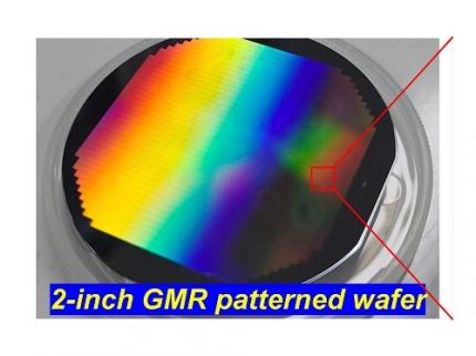
< Figure 1. Schematic diagram of the InGaAs photodiode image sensor integrated on the Guided-Mode Resonance (GMR) structure proposed in this study (left), a photograph of the fabricated wafer, and a scanning electron microscope (SEM) image of the periodic patterns (right) >
The research team introduced a guided-mode resonance (GMR) structure* that enables high-efficiency light absorption across a wide spectral range from 400 nanometers (nm) to 1,700 nanometers (nm). This wavelength range includes not only visible light but also light the SWIR region, making it valuable for various industrial applications.
*Guided-Mode Resonance (GMR) Structure: A concept used in electromagnetics, a phenomenon in which a specific (light) wave resonates (forming a strong electric/magnetic field) at a specific wavelength. Since energy is maximized under these conditions, it has been used to increase antenna or radar efficiency.
The improved performance in the SWIR region is expected to play a significant role in developing next-generation image sensors with increasingly high resolutions. The GMR structure, in particular, holds potential for further enhancing resolution and other performance metrics through hybrid integration and monolithic 3D integration with complementary metal-oxide-semiconductor (CMOS)-based readout integrated circuits (ROIC).
< Figure 2. Benchmark for state-of-the-art InGaAs-based SWIR pixels with simulated EQE lines as a function of TAL variation. Performance is maintained while reducing the absorption layer thickness from 2.1 micrometers or more to 1 micrometer or less while reducing it by 50% to 70% >
The research team has significantly enhanced international competitiveness in low-power devices and ultra-high-resolution imaging technology, opening up possibilities for applications in digital cameras, security systems, medical and industrial image sensors, as well as future ultra-high-resolution sensors for autonomous driving, aerospace, and satellite observation.
Professor Sang Hyun Kim, the lead researcher, commented, “This research demonstrates that significantly higher performance than existing technologies can be achieved even with ultra-thin absorption layers.”
< Figure 3. Top optical microscope image and cross-sectional scanning electron microscope image of the InGaAs photodiode image sensor fabricated on the GMR structure (left). Improved quantum efficiency performance of the ultra-thin image sensor (red) fabricated with the technology proposed in this study (right) >
The results of this research were published on 15th of November, in the prestigious international journal Light: Science & Applications (JCR 2.9%, IF=20.6), with Professor Dae-Myung Geum of Inha University (formerly a KAIST postdoctoral researcher) and Dr. Jinha Lim (currently a postdoctoral researcher at Yale University) as co-first authors. (Paper title: “Highly-efficient (>70%) and Wide-spectral (400 nm -1700 nm) sub-micron-thick InGaAs photodiodes for future high-resolution image sensors”)
This study was supported by the National Research Foundation of Korea.
2024.11.22 View 3620
KAIST Secures Core Technology for Ultra-High-Resolution Image Sensors
A joint research team from Korea and the United States has developed next-generation, high-resolution image sensor technology with higher power efficiency and a smaller size compared to existing sensors. Notably, they have secured foundational technology for ultra-high-resolution shortwave infrared (SWIR) image sensors, an area currently dominated by Sony, paving the way for future market entry.
KAIST (represented by President Kwang Hyung Lee) announced on the 20th of November that a research team led by Professor SangHyeon Kim from the School of Electrical Engineering, in collaboration with Inha University and Yale University in the U.S., has developed an ultra-thin broadband photodiode (PD), marking a significant breakthrough in high-performance image sensor technology.
This research drastically improves the trade-off between the absorption layer thickness and quantum efficiency found in conventional photodiode technology. Specifically, it achieved high quantum efficiency of over 70% even in an absorption layer thinner than one micrometer (μm), reducing the thickness of the absorption layer by approximately 70% compared to existing technologies.
A thinner absorption layer simplifies pixel processing, allowing for higher resolution and smoother carrier diffusion, which is advantageous for light carrier acquisition while also reducing the cost. However, a fundamental issue with thinner absorption layers is the reduced absorption of long-wavelength light.
< Figure 1. Schematic diagram of the InGaAs photodiode image sensor integrated on the Guided-Mode Resonance (GMR) structure proposed in this study (left), a photograph of the fabricated wafer, and a scanning electron microscope (SEM) image of the periodic patterns (right) >
The research team introduced a guided-mode resonance (GMR) structure* that enables high-efficiency light absorption across a wide spectral range from 400 nanometers (nm) to 1,700 nanometers (nm). This wavelength range includes not only visible light but also light the SWIR region, making it valuable for various industrial applications.
*Guided-Mode Resonance (GMR) Structure: A concept used in electromagnetics, a phenomenon in which a specific (light) wave resonates (forming a strong electric/magnetic field) at a specific wavelength. Since energy is maximized under these conditions, it has been used to increase antenna or radar efficiency.
The improved performance in the SWIR region is expected to play a significant role in developing next-generation image sensors with increasingly high resolutions. The GMR structure, in particular, holds potential for further enhancing resolution and other performance metrics through hybrid integration and monolithic 3D integration with complementary metal-oxide-semiconductor (CMOS)-based readout integrated circuits (ROIC).
< Figure 2. Benchmark for state-of-the-art InGaAs-based SWIR pixels with simulated EQE lines as a function of TAL variation. Performance is maintained while reducing the absorption layer thickness from 2.1 micrometers or more to 1 micrometer or less while reducing it by 50% to 70% >
The research team has significantly enhanced international competitiveness in low-power devices and ultra-high-resolution imaging technology, opening up possibilities for applications in digital cameras, security systems, medical and industrial image sensors, as well as future ultra-high-resolution sensors for autonomous driving, aerospace, and satellite observation.
Professor Sang Hyun Kim, the lead researcher, commented, “This research demonstrates that significantly higher performance than existing technologies can be achieved even with ultra-thin absorption layers.”
< Figure 3. Top optical microscope image and cross-sectional scanning electron microscope image of the InGaAs photodiode image sensor fabricated on the GMR structure (left). Improved quantum efficiency performance of the ultra-thin image sensor (red) fabricated with the technology proposed in this study (right) >
The results of this research were published on 15th of November, in the prestigious international journal Light: Science & Applications (JCR 2.9%, IF=20.6), with Professor Dae-Myung Geum of Inha University (formerly a KAIST postdoctoral researcher) and Dr. Jinha Lim (currently a postdoctoral researcher at Yale University) as co-first authors. (Paper title: “Highly-efficient (>70%) and Wide-spectral (400 nm -1700 nm) sub-micron-thick InGaAs photodiodes for future high-resolution image sensors”)
This study was supported by the National Research Foundation of Korea.
2024.11.22 View 3620 -
 KAIST researchers devises a technology to utilize ultrahigh-resolution micro-LED with 40% reduced self-generated heat
In the digitized modern life, various forms of future displays, such as wearable and rollable displays are required. More and more people are wanting to connect to the virtual world whenever and wherever with the use of their smartglasses or smartwatches. Even further, we’ve been hearing about medical diagnosis kit on a shirt and a theatre-hat. However, it is not quite here in our hands yet due to technical limitations of being unable to fit as many pixels as a limited surface area of a glasses while keeping the power consumption at the a level that a hand held battery can supply, all the while the resolution of 4K+ is needed in order to perfectly immerse the users into the augmented or virtual reality through a wireless smartglasses or whatever the device.
KAIST (President Kwang Hyung Lee) announced on the 22nd that Professor Sang Hyeon Kim's research team of the Department of Electrical and Electronic Engineering re-examined the phenomenon of efficiency degradation of micro-LEDs with pixels in a size of micrometers (μm, one millionth of a meter) and found that it was possible to fundamentally resolve the problem by the use of epitaxial structure engineering.
Epitaxy refers to the process of stacking gallium nitride crystals that are used as a light emitting body on top of an ultrapure silicon or sapphire substrate used for μLEDs as a medium.
μLED is being actively studied because it has the advantages of superior brightness, contrast ratio, and lifespan compared to OLED. In 2018, Samsung Electronics commercialized a product equipped with μLED called 'The Wall'. And there is a prospect that Apple may be launching a μLED-mounted product in 2025.
In order to manufacture μLEDs, pixels are formed by cutting the epitaxial structure grown on a wafer into a cylinder or cuboid shape through an etching process, and this etching process is accompanied by a plasma-based process. However, these plasmas generate defects on the side of the pixel during the pixel formation process.
Therefore, as the pixel size becomes smaller and the resolution increases, the ratio of the surface area to the volume of the pixel increases, and defects on the side of the device that occur during processing further reduce the device efficiency of the μLED. Accordingly, a considerable amount of research has been conducted on mitigating or removing sidewall defects, but this method has a limit to the degree of improvement as it must be done at the post-processing stage after the grown of the epitaxial structure is finished.
The research team identified that there is a difference in the current moving to the sidewall of the μLED depending on the epitaxial structure during μLED device operation, and based on the findings, the team built a structure that is not sensitive to sidewall defects to solve the problem of reduced efficiency due to miniaturization of μLED devices. In addition, the proposed structure reduced the self-generated heat while the device was running by about 40% compared to the existing structure, which is also of great significance in commercialization of ultrahigh-resolution μLED displays.
This study, which was led by Woo Jin Baek of Professor Sang Hyeon Kim's research team at the KAIST School of Electrical and Electronic Engineering as the first author with guidance by Professor Sang Hyeon Kim and Professor Dae-Myeong Geum of the Chungbuk National University (who was with the team as a postdoctoral researcher at the time) as corresponding authors, was published in the international journal, 'Nature Communications' on March 17th. (Title of the paper: Ultra-low-current driven InGaN blue micro light-emitting diodes for electrically efficient and self-heating relaxed microdisplay).
Professor Sang Hyeon Kim said, "This technological development has great meaning in identifying the cause of the drop in efficiency, which was an obstacle to miniaturization of μLED, and solving it with the design of the epitaxial structure.“ He added, ”We are looking forward to it being used in manufacturing of ultrahigh-resolution displays in the future."
This research was carried out with the support of the Samsung Future Technology Incubation Center.
Figure 1. Image of electroluminescence distribution of μLEDs fabricated from epitaxial structures with quantum barriers of different thicknesses while the current is running
Figure 2. Thermal distribution images of devices fabricated with different epitaxial structures under the same amount of light.
Figure 3. Normalized external quantum efficiency of the device fabricated with the optimized epitaxial structure by sizes.
2023.03.23 View 6817
KAIST researchers devises a technology to utilize ultrahigh-resolution micro-LED with 40% reduced self-generated heat
In the digitized modern life, various forms of future displays, such as wearable and rollable displays are required. More and more people are wanting to connect to the virtual world whenever and wherever with the use of their smartglasses or smartwatches. Even further, we’ve been hearing about medical diagnosis kit on a shirt and a theatre-hat. However, it is not quite here in our hands yet due to technical limitations of being unable to fit as many pixels as a limited surface area of a glasses while keeping the power consumption at the a level that a hand held battery can supply, all the while the resolution of 4K+ is needed in order to perfectly immerse the users into the augmented or virtual reality through a wireless smartglasses or whatever the device.
KAIST (President Kwang Hyung Lee) announced on the 22nd that Professor Sang Hyeon Kim's research team of the Department of Electrical and Electronic Engineering re-examined the phenomenon of efficiency degradation of micro-LEDs with pixels in a size of micrometers (μm, one millionth of a meter) and found that it was possible to fundamentally resolve the problem by the use of epitaxial structure engineering.
Epitaxy refers to the process of stacking gallium nitride crystals that are used as a light emitting body on top of an ultrapure silicon or sapphire substrate used for μLEDs as a medium.
μLED is being actively studied because it has the advantages of superior brightness, contrast ratio, and lifespan compared to OLED. In 2018, Samsung Electronics commercialized a product equipped with μLED called 'The Wall'. And there is a prospect that Apple may be launching a μLED-mounted product in 2025.
In order to manufacture μLEDs, pixels are formed by cutting the epitaxial structure grown on a wafer into a cylinder or cuboid shape through an etching process, and this etching process is accompanied by a plasma-based process. However, these plasmas generate defects on the side of the pixel during the pixel formation process.
Therefore, as the pixel size becomes smaller and the resolution increases, the ratio of the surface area to the volume of the pixel increases, and defects on the side of the device that occur during processing further reduce the device efficiency of the μLED. Accordingly, a considerable amount of research has been conducted on mitigating or removing sidewall defects, but this method has a limit to the degree of improvement as it must be done at the post-processing stage after the grown of the epitaxial structure is finished.
The research team identified that there is a difference in the current moving to the sidewall of the μLED depending on the epitaxial structure during μLED device operation, and based on the findings, the team built a structure that is not sensitive to sidewall defects to solve the problem of reduced efficiency due to miniaturization of μLED devices. In addition, the proposed structure reduced the self-generated heat while the device was running by about 40% compared to the existing structure, which is also of great significance in commercialization of ultrahigh-resolution μLED displays.
This study, which was led by Woo Jin Baek of Professor Sang Hyeon Kim's research team at the KAIST School of Electrical and Electronic Engineering as the first author with guidance by Professor Sang Hyeon Kim and Professor Dae-Myeong Geum of the Chungbuk National University (who was with the team as a postdoctoral researcher at the time) as corresponding authors, was published in the international journal, 'Nature Communications' on March 17th. (Title of the paper: Ultra-low-current driven InGaN blue micro light-emitting diodes for electrically efficient and self-heating relaxed microdisplay).
Professor Sang Hyeon Kim said, "This technological development has great meaning in identifying the cause of the drop in efficiency, which was an obstacle to miniaturization of μLED, and solving it with the design of the epitaxial structure.“ He added, ”We are looking forward to it being used in manufacturing of ultrahigh-resolution displays in the future."
This research was carried out with the support of the Samsung Future Technology Incubation Center.
Figure 1. Image of electroluminescence distribution of μLEDs fabricated from epitaxial structures with quantum barriers of different thicknesses while the current is running
Figure 2. Thermal distribution images of devices fabricated with different epitaxial structures under the same amount of light.
Figure 3. Normalized external quantum efficiency of the device fabricated with the optimized epitaxial structure by sizes.
2023.03.23 View 6817